PCB Copper Plating - One of the most expensive processes
28 October 2023
Views: 819
What is the function of PCB copper plating?
Copper plating is a process that uses chemical formaldehyde under strong alkaline conditions of potassium permanganate to oxidize and reduce chemical copper ions, depositing a layer of 0.3um-0.5um copper on the inner wall of the hole, making the originally non-conductive hole wall conductive. This facilitates subsequent processes such as surface and pattern electroplating, enabling the same layer to be thickened to the thickness required by customers, thus achieving effective electrical connection between the circuits on the PCB.
What is the process of PCB copper plating?
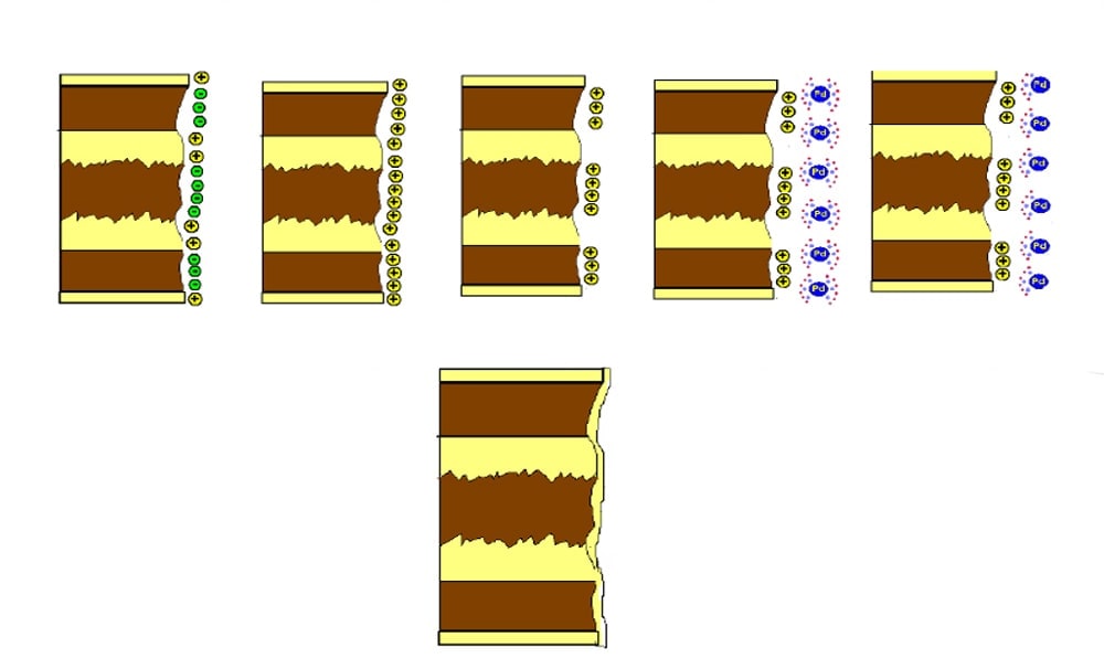
Oil removal and hole treatment: clean the surface and adjust the electrical properties of the hole wall.
Micro-etching: roughen the copper surface and remove oxides.
Pre-immersion: prevent impurities such as water and copper ions from entering the palladium tank; enhance the immersion of the hole.
Activation: adsorb colloidal palladium to provide a catalyst for copper plating.
Desmear: remove the Sn4 shell on the outer layer of the colloidal palladium and remove loose colloidal particles.
Copper plating: using palladium atoms as a catalyst, deposit a layer of copper on the hole wall to achieve interconnection between layers.
Why is copper plating one of the most expensive processes in PCB manufacturing?
High raw material cost: Copper plating requires the use of high-purity copper solution, which is very expensive and typically several times or even tens of times more expensive than other plating solutions. Other materials such as electrolytes and photoresist coatings are also similarly expensive.
Labor cost: PCB copper plating requires multiple processing steps, each of which requires highly skilled workers, so a significant amount of labor cost is needed.
Long production cycle: Copper plating requires multiple chemical reactions and heat treatments, which lengthens the production cycle and increases manufacturing costs.
High technical difficulty: The copper plating process requires strict control of parameters such as temperature, concentration, and pH value, and the control of these parameters requires high technical skills from the operators, making it easy to make mistakes.
High equipment cost: Copper plating requires specialized equipment and processes, and the cost of these equipment is also relatively high.

PCB copper plating is an important step in PCB manufacturing because it enables circuit connection, current transmission, and signal transmission. Compared with traditional mechanical processing methods, PCB copper plating can achieve PCB design more accurately and efficiently, so the copper plating process can produce very fine, high-density printed circuit boards, making it widely used in the manufacturing process of high-end electronic products.


