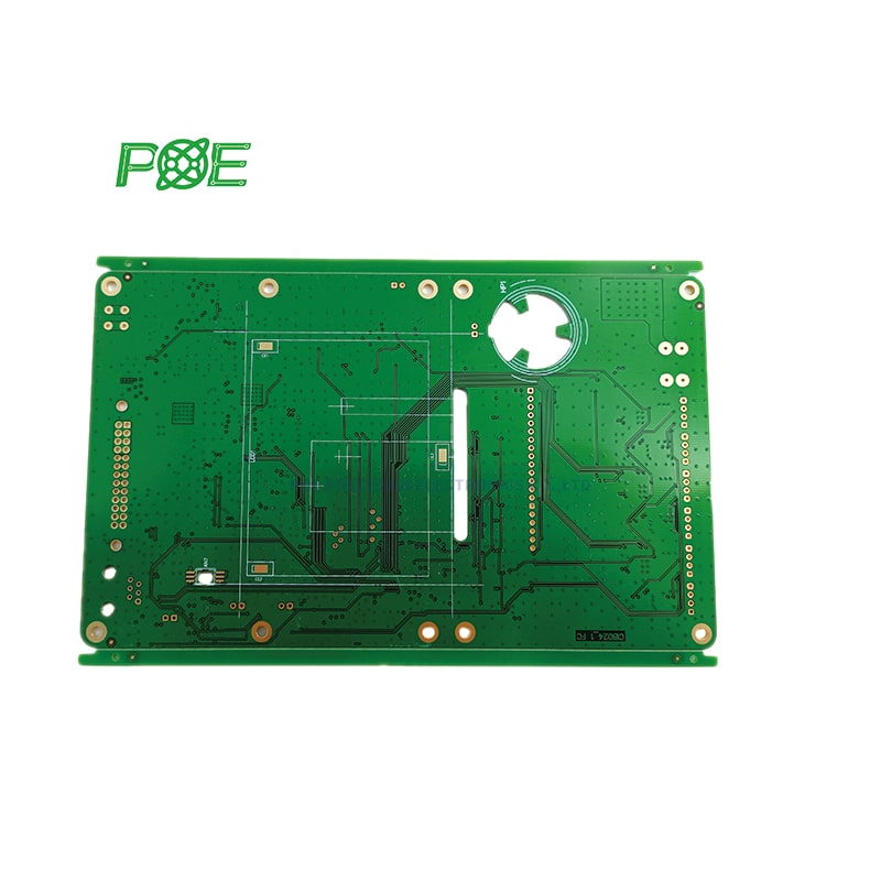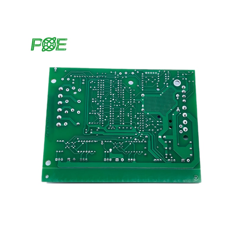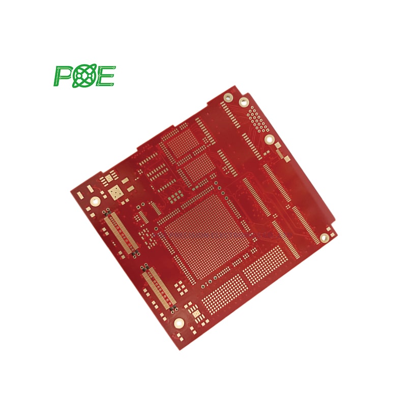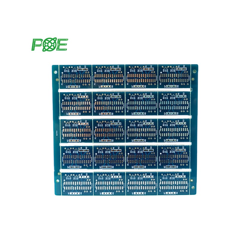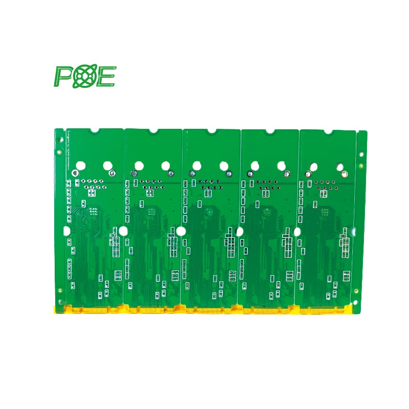
China 1-40layer PCB/PCBA/EMS/OEM
One stop contract Manufacturing facility
One stop contract Manufacturing facility


+8613798543496


| Layers | 1-40+ layers |
| Materials | FR-4 (standard), FR-4 High-Tg, Aluminum, Rogers, and other special materials |
| Board Thickness | 0.2mm – 6mm |
| Copper Thickness | 1/3 Oz (12 µm) – 6 Oz (210 µm), depends on design and material requirements |
| Minimum Trace Width/Spacing | 3mil/3mil (0.0762mm/0.0762mm) or better, depending on design and materials |
| Minimum Hole Size | 0.2mm (8mil) or larger |
| Aspect Ratio | 10:1 or higher |
| Max Board Size | Typically up to 600mm x 1200mm or larger |
| Surface Finish | ENIG, Immersion Silver, OSP, HASL, Lead-Free HASL, ENEPIG, Hard Gold (finger), etc. |
| Solder Mask | Green, Blue, Yellow, Black, Red, White, and other colors |
| Solder Mask Resolution | 4mil (0.1mm) minimum |
| Solder Mask Registration | ±2mil (±0.0508mm) |
| Silkscreen Color | White, Black, Yellow, Blue, Red |
| Plated Through Holes (PTH) |
Yes |
| Blind & Buried Vias (BBV) |
Yes |
| Via-in-Pad |
Yes, filled and capped vias |
| Controlled Impedance |
Yes, can be achieved in single-ended or differential pairs, depending on material, stack-up, and trace geometry |
| Routing & Scoring |
V-groove (V-cut), Tab-routing (mouse bites), and individual routing |
| Electrical Testing |
Continuity & isolation, impedance control, Hi-Pot, etc. |
| Mechanical Assembly |
Supported |
| Special Routing Features |
Castellated holes, countersinks, counterbores, slots, and notched routes |
| Certification | ISO9001:2015;ISO13485:2016;ROHS,UL 94v0, IPC-600G classll and IPC-6012B classll standard |

*If you need bare PCB manufacturing + component assembly, then you need to provide gerber file and bom.

Email: all@poe-pcba.com

Since 1996, POE has become a globally renowned PCB company, providing small to medium volume PCB/ PCBA manufacturing services.