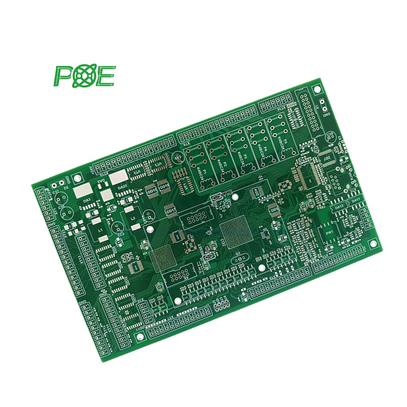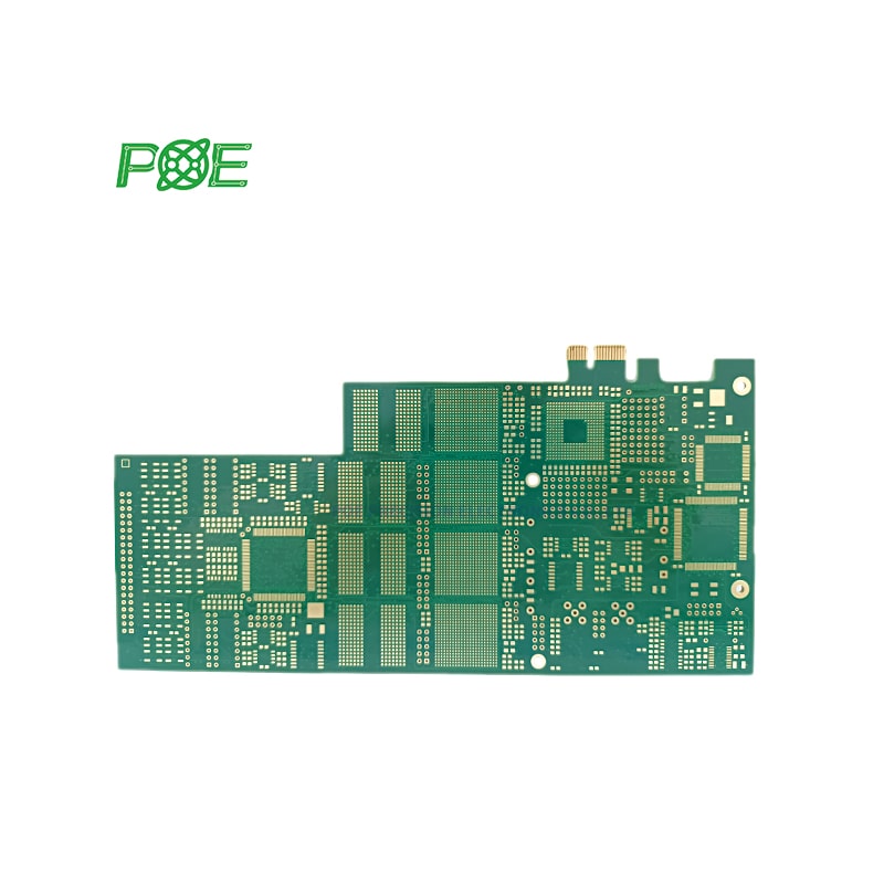
China 1-40layer PCB/PCBA/EMS/OEM
One stop contract Manufacturing facility
One stop contract Manufacturing facility


+8613798543496


☞ Turnaround time: 1-4 days;
☞ Small to Medium Volume;
☞ Rigid, Flexible, HDI PCB;
☞ MOQ: 100pcs.

☞ Lead Time: 1-7days;
☞ Global Sourcing of Components;
☞ Full turnkey, partial turnkey;
☞ MOQ: 100pcs.
We respect customer's copyright and will never manufacture PCBs for someone else with your files unless we receive written permission from you, nor we'll share these files with any other 3rd parties.
Yes.
We can process Gerber RS-274X, ODB++ files, PCB file and BRD files.
No, as these formats do not translate to our PCB Fabrication machinery.
Yes.
If you encounter any defects or quality issues with the PCB upon receiving it and are unsatisfied, please inform us at all@poe-pcba.com. We will repair or remake your PCB, and we will respond within 8 hours until you are satisfied.

Since 1996, POE has become a globally renowned PCB company, providing small to medium volume PCB/ PCBA manufacturing services.