1. Design requirements analysis: Before PCB design, we will understand the needs and requirements of customers, including circuit function, performance, purpose, budget, analyze circuit parameters, PCB size, components, number of layers, process requirements, etc., for follow-up design work.
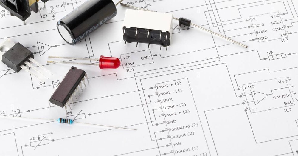
2. Schematic diagram design: Before circuit board design, use schematic design software tools to draw the schematic diagram of the circuit, and use Altium Designer, Eagle, etc. to design the schematic diagram to better understand the circuit structure and function.
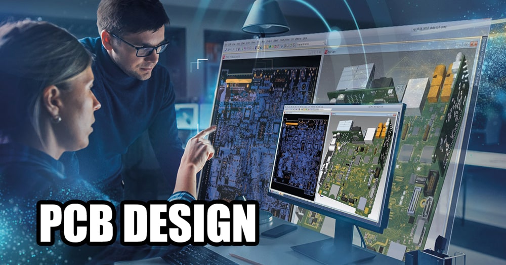
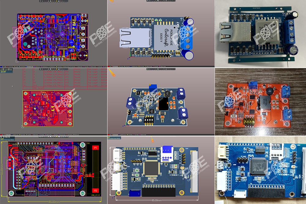
3. PCB layout design: After the schematic design, PCB layout design is required. Layout design involves placing circuit components where to place them on the board and determining how they are connected. In the layout design, factors such as the size of the circuit board, the size and location of the device, the number of layers of the circuit board, signal traces, power supply and ground wires need to be considered.
4. Generate PCB production files: convert the designed circuit board into manufacturing files, including Gerber files, drilling files, BOM (Bill of Materials, bill of materials), etc., for processing and manufacturing during the PCB manufacturing process.
5. PCB prototype manufacturing: Send the Gerber file to the PCB manufacturer for PCB prototype manufacturing, assembly and testing.
6. PCB test: test the manufactured circuit board, including power test, signal test, noise test, etc., to ensure that the performance and reliability of the circuit board meet the requirements.
7. PCB debugging and modification: According to the test results, debug and modify the circuit board to optimize the performance and reliability of the circuit board.
8. Final confirmation and delivery: After testing and modification, the performance and reliability of the circuit board are finally confirmed to meet the requirements, and shipped to the customer.


