China 1-40layer PCB/PCBA/EMS/OEM
One stop contract Manufacturing facility
One stop contract Manufacturing facility


+8613798543496


Consumer electronics have become an essential part of our daily lives. From smartphones and tablets to smartwatches and fitness trackers, we rely on these devices to stay connected, entertained, and informed. Behind the sleek designs and advanced features of these products lies a complex web of electronics, including the printed circuit board. PCB design plays a critical role in the success of many consumer electronics products, as it determines the functionality, performance, and reliability of the device. In this article, we will explore the latest trends and innovations in PCB design for consumer electronics.

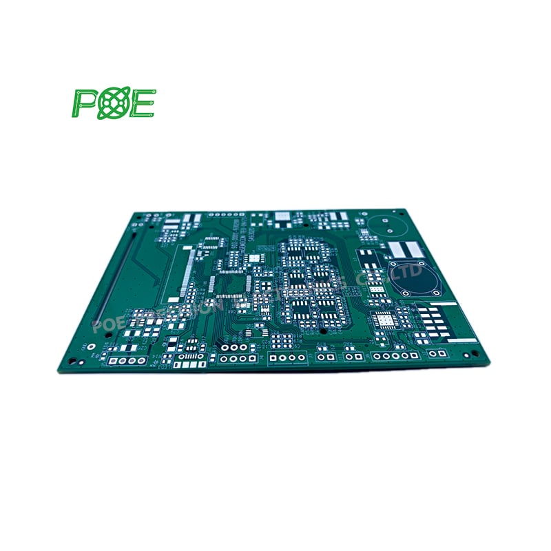
One of the most significant trends in consumer electronics is miniaturization. Consumers expect their devices to be smaller, thinner, and more portable than ever before. This presents unique challenges for PCB designers, who must pack more functionality into a smaller footprint. To meet these demands, designers are using advanced techniques such as high-density interconnect (HDI) and multilayer PCBs.

HDI PCBs are designed to maximize the use of space on the PCB. They use a combination of through-hole vias, blind vias, and buried vias to connect multiple layers of the PCB. This allows designers to pack more components into a smaller areas, while also improving signal integrity and reducing noise.
Multilayer PCBs are another popular choice for miniaturization. These PCBs have multiple layers of copper tracks separated by insulating layers. They allow designers to add more components and traces to the PCB, without increasing its size. Multilayer PCBs also provide better signal integrity and reduce electromagnetic interference (EMI).
In addition to these techniques, designers are also using smaller components, such as surface-mounted devices (SMDs), to save space on the PCB. SMDs are mounted directly onto the surface of the PCB, without the need for leads or wires, which reduces the overall size of the component. These components are also more reliable and have better thermal performance than traditional through-hole components.
Flexible PCBs are becoming increasingly popular in consumer electronics products, as they offer greater design flexibility and can be used in a variety of form factors. These PCBs are made from flexible materials such as polyimide and can be bent or twisted without breaking. They are particularly useful in wearables and other portable devices, where flexibility is essential.

Flexible PCBs can be designed in a variety of shapes and sizes, which allows designers to create products with unique form factors. They can also be used to connect different components within a device, creating a flexible and modular design. For example, a flexible PCB could be used to connect the display, battery, and other components in a smartwatch, creating a more compact and streamlined design.
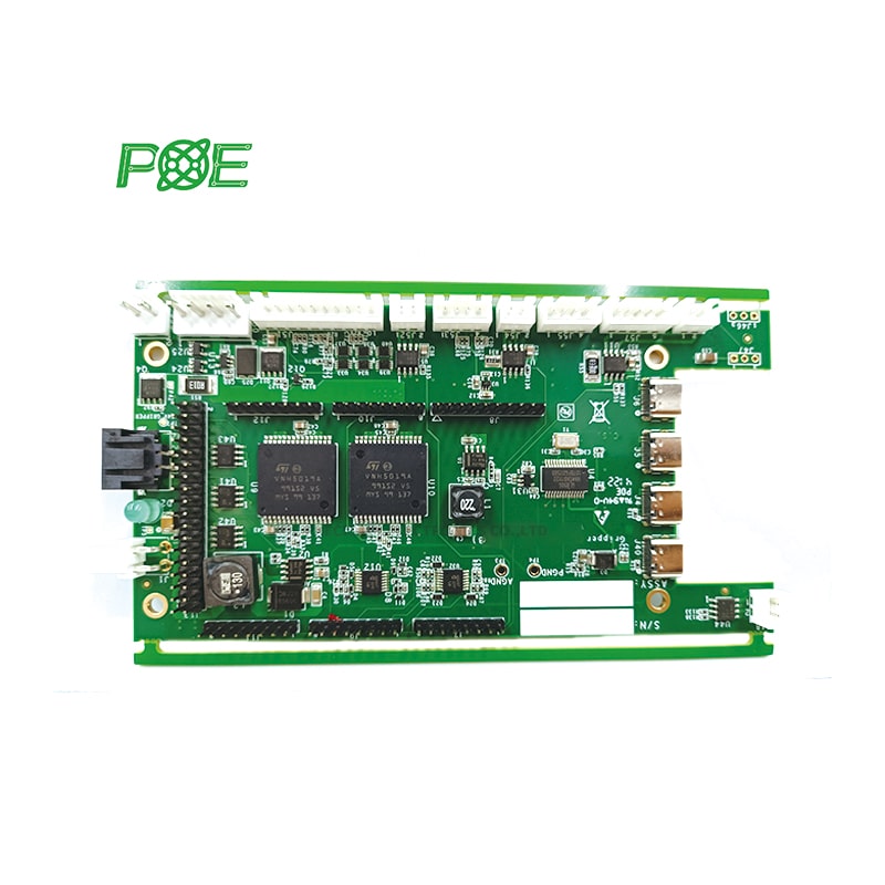
Wireless connectivity has become a standard feature in many consumer electronics products, driven by the rise of Internet of Things (IoT) devices. PCB designers are incorporating wireless modules into their designs, such as Wi-Fi, Bluetooth, and cellular connectivity, to enable seamless communication between devices.

To ensure reliable wireless connectivity, PCB designers must pay close attention to the placement and orientation of antennas on the PCB. Antennas should be placed away from sources of interference, such as metal components or other antennas, and oriented in the correct direction for optimal signal strength. Designers must also consider the impact of the PCB layout on signal integrity, as noise and interference can degrade wireless performance.
Battery life is a crucial factor in the user experience of consumer electronics products. PCB designers are incorporating power-efficient design techniques to extend battery life and reduce power consumption. These techniques include minimizing power consumption during standby mode, optimizing voltage regulators, and using low-power components.
Designers can also use power management ICs (PMICs) to control the power consumption of the device. PMICs can regulate the voltage and current supply to different components, ensuring that they operate at the optimal level of power consumption. This can help extend battery life and reduce power consumption, while still maintaining the performance and functionality of the device.
Sensors are becoming more prevalent in consumer electronics products, allowing devices to collect data about their environment and provide better user experiences. PCB designers are incorporating sensors directly into their designs, such as temperature sensors, accelerometers, and gyroscopes, to provide valuable data to the device.

In addition to traditional sensors, designers are also incorporating new types of sensors into their designs, such as biometric sensors and environmental sensors. Biometric sensors, such as heart rate monitors and fingerprint sensors, are becoming more common in wearable devices, while environmental sensors, such as air quality sensors and humidity sensors, are being used in smart home devices.
Environmental considerations are becoming increasingly important in the design of consumer electronics products. PCB designers are using eco-friendly materials, such as lead-free and halogen-free PCBs, to reduce the environmental impact of their products. They are also designing products with longer lifespans, reducing the need for frequent replacements and disposals.
PCB manufacturers are adopting advanced manufacturing techniques to keep up with the demands of the consumer electronics industry. One of these techniques is automated assembly, which uses robots and other machines to assemble PCBs quickly and accurately. This reduces the time and cost of PCB production, while improving the quality and consistency of the finished product.
Another advanced manufacturing technique is automated inspection, which uses machines to inspect PCBs for defects and errors. This helps ensure that the PCB meets the required quality standards, while reducing the risk of human error.
As consumer electronics devices become more powerful and complex, high-speed design has become a crucial consideration for PCB designers. High-speed design refers to the design of PCBs that operate at high frequencies, typically above 1 GHz. These PCBs require careful attention to signal timing, impedance matching, and noise reduction to ensure reliable performance.

To achieve high-speed design, designers must use specialized design software and simulation tools to model the behavior of signals on the PCB. They must also carefully select components, such as high-speed connectors and high-speed memory, that can handle high-frequency signals. Designers must also consider the impact of the PCB layout on signal integrity, as even small changes in the layout can affect signal timing and noise.
As consumer electronics devices become more connected and collect more data, security has become a critical consideration for PCB designers. Designers must ensure that their products are secure from hacking and other cyber threats, to protect the privacy and security of users.
One way that designers are addressing this issue is by incorporating hardware security features directly into the PCB design. These features can include secure booting, secure storage, and secure communication, which help protect the device from unauthorized access and tampering. Designers must also consider the impact of the PCB layout on security, as the layout can affect the physical security of the device and the effectiveness of security features.
PCB design is a critical component of consumer electronics products. By embracing the latest trends and innovations, PCB designers can create products that are more powerful, efficient, and environmentally friendly than ever before. From miniaturization and flexibility to wireless connectivity and power efficiency, these trends are shaping the future of consumer electronics. As the industry continues to evolve, PCB designers must stay up-to-date with the latest developments to create products that meet the changing needs of consumers.
If you have consumer electronics PCB design, manufacturing, and assembly needs, please feel free to contact us. We, POE, have more than 20 years of experience in the PCB industry and can design and manufacture the most advanced PCBs for you.

Since 1996, POE has become a globally renowned PCB company, providing small to medium volume PCB/ PCBA manufacturing services.